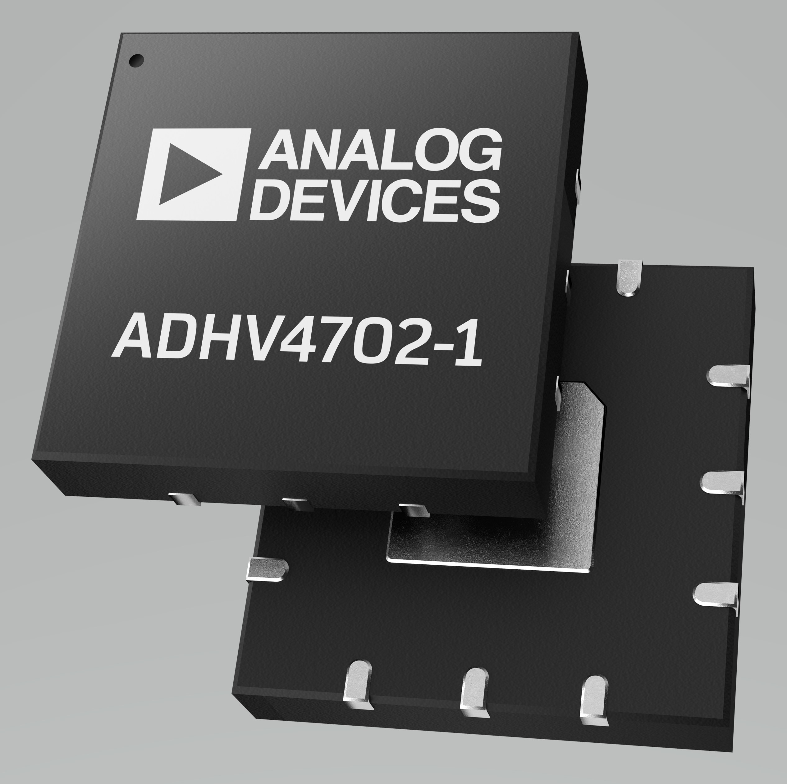
Analog DevicesADHV4702-1BCPZ-R7OP-Amp
Op Amp Single Precision Amplifier ±110V/220V 12-Pin LFCSP EP T/R
The ADHV4702-1 is a high voltage (220 V), unity-gain stable precision operational amplifier. The ADHV4702-1 offers high input impedance with low input bias current, low input offset voltage, low drift, and low noise for precision demanding applications. The next generation of proprietary semiconductor processes and innovative architecture from Analog Devices, Inc., enable this precision operational amplifier to operate from symmetrical dual supplies of ±110 V, asymmetrical dual supplies, or a single supply of 220 V.
precision performance, the ADHV4702-1 has a 170 dB typical open-loop gain (AOL) and a 160 dB typical common-mode rejection ratio (CMRR). The ADHV4702-1 also has a 2 μV/°C maximum input offset voltage (VOS) drift and an 8 nV/√Hz input voltage noise.
The exceptional dc precision of the ADHV4702-1 is complemented by excellent dynamic performance with a small signal bandwidth of 10 MHz and a slew rate of 74 V/μs. The ADHV4702-1 has an output current of 20 mA typical.
The ADHV4702-1 offers high voltage input common-mode swing as well as high voltage output swing, enabling precision high voltage use cases such as high-side current sensing. The ADHV4702-1 is also ideally suited for forcing a voltage in precision bias and control applications.
The ADHV4702-1 is available in a 12-lead, 7 mm × 7 mm lead frame chip scale package (LFCSP) with an exposed pad (EPAD) compliant to international electrotechnical commission (IEC) 61010-1 creepage and clearance standards. The copper EPAD provides a low thermal resistance path to improve heat dissipation and features high voltage isolation, allowing it to be safely connected to a 0 V ground plane regardless of VCC or VEE voltages. The ADHV4702-1 operates over the −40°C to +85°C industrial temperature range.
Features and Benefits:
- Wide range of operating voltages
- Dual-supply: ±12 V to ±110 V
- Asymmetrical supply operation: 24 V to 220 V
- Wide input common-mode voltage range: 3 V from rails
- High common-mode rejection ratio: 160 dB typical
- High AOL: 170 dB typical
- High slew rate
- 74 V/μs typical
- 24 V/μs typical with external input clamping diodes
- Low input bias current: 2 pA maximum
- Low input offset voltage: 1 mV maximum
- Low input offset voltage drift: 2 μV/°C maximum
- Low input voltage noise: 8 nV/√Hz typical at 10 kHz
- Wide small signal bandwidth: 10 MHz typical
- Resistor adjustable quiescent current: 0.6 mA to 3 mA (VS = ±110 V)
- Unity-gain stable
- Thermal monitoring
- Small footprint: 12-lead, 7 mm × 7 mm LFCSP compliant with IEC 61010-1 spacing
- Shutdown mode
Applications:
- High-side current sensing
- Automated test equipment
- High voltage drivers
- Piezotransducers
- Digital-to-analog converter (DAC) output buffers
- Light detecting and ranging (LiDAR), avalanche photodiode (APD), single photon avalanche diode (SPAD) biasing
Product Lifecycle: Recommended for new designs. This product has been released to the market. The data sheet contains all final specifications and operating conditions. For new designs, ADI recommends utilization of these products.
| Compliant | |
| EAR99 | |
| Active | |
| 8542.33.00.01 | |
| Automotive | No |
| PPAP | No |
| Befestigung | Surface Mount |
| Verpackungshöhe | 0.73 mm |
| Verpackungsbreite | 7 mm |
| Verpackungslänge | 7 mm |
| Leiterplatte geändert | 12 |
| Standard-Verpackungsname | CSP |
| Lieferantenverpackung | LFCSP EP |
| 12 |
